EM74LVC1G00
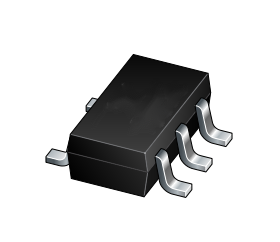
Single 2-input NAND gate-EM74LVC1G00
Product details
| Technology family | LVC |
| Supply voltage (min) (V) | 1.65 |
| Supply voltage (max) (V) | 5.5 |
| Number of channels | 1 |
| Inputs per channel | 1 |
| IOL (max) (mA) | 32 |
| IOH (max) (mA) | -32 |
| Input type | Standard CMOS |
| Output type | Push-Pull |
| Features | Over-voltage tolerant inputs, Partial power down (Ioff), Ultra high speed (tpd <5ns) |
| Data rate (max) (MBps) | 100 |
| Rating | Catalog |
| Operating temperature range (°C) | -40 to 125 |
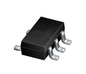
| EM74LVC1G00GV | SOT23-5L | SOT23 package, 5 pins 2.92 mm × 1.6 mm; 1.25 mm (Max) height |
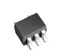
| EM74LVC1G00GW | SOT353 | SOT353 package, 5 pins 2.1 mm × 1.25 mm; 1.1 mm (Max) height |
| EM74LVC1G00GS | DFN1x1-6L | DFN1×1 package, 6 pins 1 mm × 1 mm; 0.42 mm (Max) height |
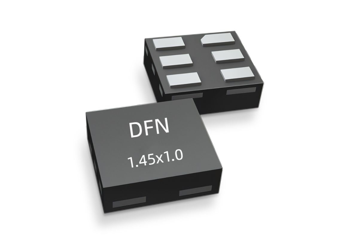
| EM74LVC1G00GM | DFN1x1.45-6L | DFN1.45×1 package, 6 pins1.45 mm × 1 mm; 0.6 mm (Max) height |
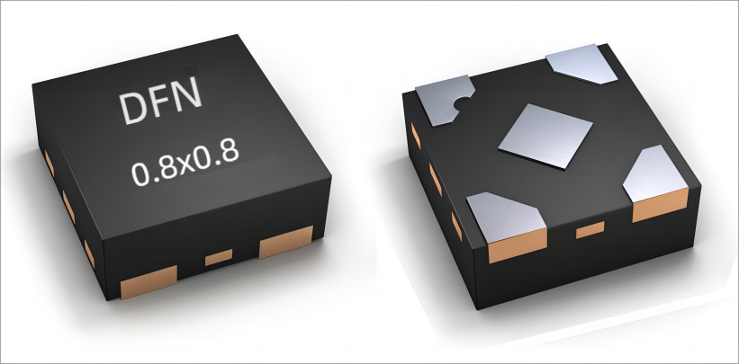
| EM74LVC1G00GX | DFN0.8x0.8-4L | DFN0.8×0.8 package, 5pins 0.8 mm × 0.8 mm; 0.4 mm (Max) height 3000 |
- Wide supply voltage range from 1.65 V to 5.5 V
- Overvoltage tolerant inputs to 5.5 V
- High noise immunity
- CMOS low power dissipation
- IOFF circuitry provides partial Power-down mode operation
- ±24 mA output drive (VCC = 3.0 V)
- Latch-up performance exceeds 100 mA
- Direct interface with TTL levels
- Complies with JEDEC standard:
- • JESD8-7 (1.65 V to 1.95 V)
- • JESD8-5 (2.3 V to 2.7 V)
- • JESD8C (2.7 V to 3.6 V)
- • JESD36 (4.5 V to 5.5 V)
- ESD protection:
- • HBM ANSI/ESDA/JEDEC JS-001 Class 3B exceeds 8000 V
- • MM JESD22-A115C Class C exceeds 550 V
- • CDM ANSI/ESDA/JEDEC JS-002 Class C3 exceeds 2000 V
- Multiple package options
The EM74LVC1G00 is a single 2-input NAND gate. Inputs can be driven from either 3.3 V or 5 V devices. This feature allows the use of these devices as translators in mixed 3.3 V and 5 V environments. Schmitt-trigger action at all inputs makes the circuit tolerant of slower input rise and fall times. This device is fully specified for partial power down applications using IOFF. The IOFF circuitry disables the output, preventing the potentially damaging backflow current through the device when it is powered down.
Similar products that you may be interested in
Functionally superior to comparative devices, can be directly replaced
This product has been launched and is available for purchase. Newer alternatives to certain products can be provided.
Single inverter-EM74LVC1G04
Design and Development
| Encapsulation | Pin Count | Download |
|---|


