咨询电话0551-6530 6032
产品详情
| Technology family | LVC |
| Supply voltage (min) (V) | 3.3 |
| Supply voltage (max) (V) | 5 |
| IOL (max) (mA) | 32 |
| Supply current (max) (µA) | 4 |
| IOH (max) (mA) | -32 |
| Input type | Schmitt-Trigger |
| Operating temperature range (°C) | -40 to 125 |
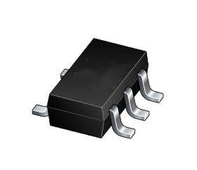
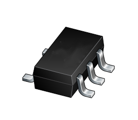
| EM74LVC2G16GV | SOT23-6L | SOT23 package, 6 pins 2.92 mm × 1.6 mm; 1.25 mm (Max) height |
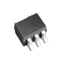
| EM74LVC2G16GW | SOT363 | SOT363 package, 6 pins 2.1 mm × 1.25 mm; 1.1 mm (Max) height |
| EM74LVC2G16GS | DFN1x1-6L | DFN1×1 package, 6 pins 1 mm × 1 mm; 0.42 mm (Max) height |
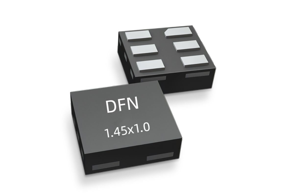
| EM74LVC2G16GM | DFN1x1.45-6L | DFN1.45×1 package, 6 pins 1.45 mm × 1 mm; 0.6 mm (Max) height |
- Wide supply voltage range from 1.65 V to 5.5 V
- Overvoltage tolerant inputs to 5.5 V
- High noise immunity
- ±24 mA output drive (VCC = 3.0 V)
- CMOS low power dissipation
- Direct interface with TTL levels
- IOFF circuitry provides partial Power-down mode operation
- Latch-up performance exceeds 100 mA
- Complies with JEDEC standard:
- • JESD8-7 (1.65 V to 1.95 V)
- • JESD8-5 (2.3 V to 2.7 V)
- • JESD8C (2.7 V to 3.6 V)
- • JESD36 (4.6 V to 5.5 V)
- ESD protection:
- • HBM ANSI/ESDA/JEDEC JS-001 Class 3B exceeds 8000 V
- • MM JESD22-A115C Class C exceeds 550 V
- • CDM ANSI/ESDA/JEDEC JS-002 Class C3 exceeds 2000 V
- Multiple package options
The EM74LVC2G16 is a dual buffer. Inputs can be driven from either 3.3 V or 5 V devices. This feature allows the use of these devices as translators in mixed 3.3 V and 5 V environments. Schmitt-trigger action at all inputs makes the circuit tolerant of slower input rise and fall times. This device is fully specified for partial power-down applications using IOFF. The IOFF circuitry disables the output, preventing the damaging backflow current through the device when it is powered down.


